Sapphire Wafers
Product Highlights
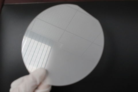 HTOT has a full wafering line and can deliver wafer sustrates or completely finished wafers to the specifications outlined below.
All wafers are produced from low stress high purity, LED grade HEM grown sapphire with a uniform crystalline structure, free of subgrains, bubbles and inclusions. This results in superior performance in downstream MOCVD processing with thin films and increased yields.
Technical Specifications
| 2” Wafer | 4” Wafer | 6” Wafer | |
| Material | >99.999% Al2O3 | >99.999% Al2O3 | >99.999% Al2O3 |
| Orientation | (C-A) ±0.1° / (C-M) ±0.1° | (C-A) ±0.1° / (C-M) ±0.1° | (C-A) ±0.1° / (C-M) ±0.1° |
| Primary Flat Location | A-axis ±0.2° | A-axis ±0.2° | A-axis ±0.2° |
| Diameter | 50± 0.05mm | 100± 0.1mm | 150± 0.2mm |
| Thickness | 430 μm ± 10μm | 650 μm ± 20μm | |
| Primary Flat Length | 16 ± 0.5mm | 16 ± 0.5mm | 16 ± 0.5mm |
| TTV | ≤5μm | ≤10μm | |
| BOW | -6~0μm | -10~0μm | |
| Warp | ≤8μm | ≤15μm | |
| LTV (5x5) | <1μm | <1.5μm | |
| Front Surface | Ra < 0.2nm, epi-ready polished | Ra < 0.2nm, epi-ready polished | Ra < 0.2nm, epi-ready polished |
| Back Surface | Ra = 1.0nm ± 0.2μm | Ra = 1.0nm ± 0.2μm | Ra = 1.0nm ± 0.2μm |
| Edge Status | No broken edge | No broken edge | No broken edge |
| Package | Clean Room, Nitrogen Atmosphere | Clean Room, Nitrogen Atmosphere | Clean Room, Nitrogen Atmosphere |
This document is copyright © September 1, 2015 GHTOT. All rights reserved. This document is provided for information purposes only; contents are subject to change without notice. It is not warranted to be error-free, nor subject to any other warranties or conditions including implied warranties and conditions of merchantability or fitness for a particular purpose.


